(China (Mainland))

Product Summary
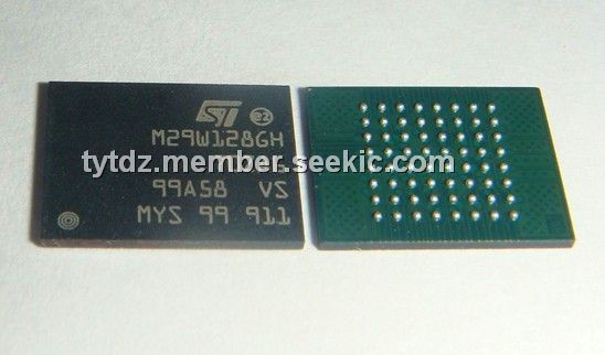
The M29W128GH70ZA6 is the 128 Mbit (8 Mb x 16 or 16 Mb x 8) non-volatile Flash memory that can be read, erased and reprogrammed. These operations can be performed using a single low voltage (2.7 to 3.6 V) supply. On power-up the M29W128GH70ZA6 memory defaults to its Read mode. The M29W128GH70ZA6 memory array is divided into 64-Kword/128-Kbyte uniform blocks that can be erased independently so it is possible to preserve valid data while old data is erased. Program and Erase commands of the M29W128GH70ZA6 are written to the command interface of the memory. An on-chip Program/Erase controller simplifies the process of programming or erasing the memory by taking care of all of the special operations that are required to update the memory contents. The end of a program or erase operation can be detected and any error conditions identified. The command set required to control the memory is consistent with JEDEC standards.
Parametrics
M29W128GH70ZA6 absolute maximum ratings: (1)Temperature under bias:- 50 to 125 ℃; (2)Storage temperature:- 65 to 150 ℃; (3)Input or output voltage(1)(2): -0.6 to VCC +0.6 V; (4)Supply voltage: - 0.6 to 4 V; (5)Input/output supply voltage: - 0.6 to 4 V; (6)Identification voltage: - 0.6 to 13.5 V; (7)Program voltage: - 0.6 to 13.5 V.
Features
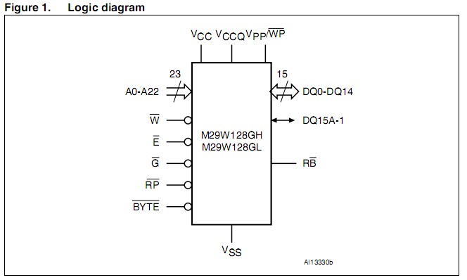
M29W128GH70ZA6 features: (1)Supply voltage: VCC = 2.7 to 3.6 V for Program, Erase and ; (2)Read; VCCQ = 1.65 to 3.6 V for I/O buffers; VPPH = 12 V for Fast Program (optional); (3)Asynchronous Random/Page Read: Page size: 8 words or 16 bytes; Page access: 25, 30 ns; Random access: 60 (only available upon customer request) or 70, 80 ns; (4)Fast Program commands: 32 words (64-byte write buffer); (5)Enhanced Buffered Program commands: 256 words; (6)Programming time: 16 μs per byte/word typical; Chip program time: 5 s with VPPH and 8 s without VPPH; (7)Memory organization: M29128GH/L: 128 main blocks, 128 Kbytes/64 Kwords each; (8)Program/Erase controller: Embedded byte/word program algorithms; (9)Program/ Erase Suspend and Resume: Read from any block during Program Suspend; Read and Program another block during Erase Suspend; (10)Unlock Bypass/Block Erase/Chip Erase/Write to Buffer/Enhanced Buffered Program commands.
Diagrams
 |
 M29W002BB |
Other |
|
Data Sheet |
Negotiable |
|
||||
|
M29W002BT |
Other |
|
Data Sheet |
Negotiable |
|
||||
|
M29W004B |
Other |
|
Data Sheet |
Negotiable |
|
||||
|
M29W004BB |
Other |
|
Data Sheet |
Negotiable |
|
||||
|
M29W004BB120N1 |
STMicroelectronics |
Flash 4M (512Kx8) 120ns |
Data Sheet |
Negotiable |
|
||||
|
M29W004BB55N1 |
STMicroelectronics |
Flash TSOP-40 512KX8 55NS |
Data Sheet |
Negotiable |
|
||||